PCB Design for Manufacturability: Best Practices for Blind and Buried ViasAuthor : Adrian September 19,pick and place solder paste dispenser 2025Table of ContentsIn the world of printed circuit board (PCB) design, achieving manufacturability while maintaining high performance is a top priority. When it comes to complex designs like High-Density Interconnect (HDI) PCBs, the use of blind and buried vias is essential for saving space and improving functionality. But how do you ensure these vias are designed for efficient production without compromising quality? This guide from ALLPCB dives deep into best practices for designing blind vias, buried vias, and microvias, focusing on manufacturability considerations, aspect ratio, and the plating process. Whether you're an engineer working on compact electronics or a designer aiming to optimize multilayer boards, this blog will walk you through actionable tips to streamline your PCB design process. Let's explore the key concepts and strategies to make your designs both innovative and production-ready.
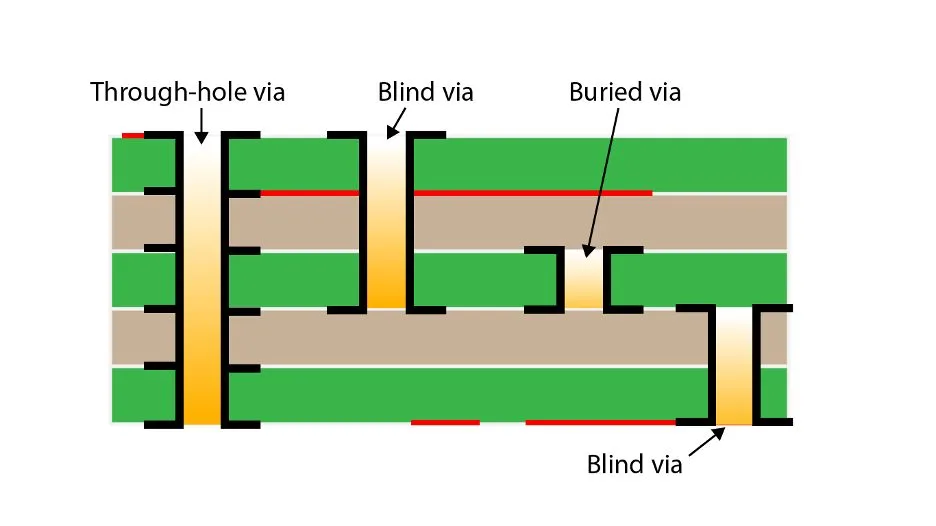
What Are Blind and Buried Vias in PCB Design?Before diving into best practices, it's important to understand the basics of blind and buried vias, especially in the context of HDI PCBs. These vias are specialized connections that help route signals between layers in multilayer boards without occupying unnecessary space on the surface.
These via types are critical for modern electronics, where devices are shrinking in size while demanding more functionality. However, their design and implementation come with unique challenges that can impact manufacturability. Let's break down the key considerations to ensure your PCB design is production-friendly.
Why Manufacturability Matters in PCB Design with Blind and Buried ViasDesigning a PCB with blind and buried vias without considering manufacturability can lead to production delays, higher costs, and even board failures. Manufacturability refers to how easily and reliably a design can be produced using standard fabrication processes. For HDI PCBs with complex via structures, overlooking this aspect can result in issues like incomplete plating, drilling errors, or thermal stress during assembly. By focusing on design for manufacturability (DFM), you can minimize these risks. This means aligning your design with the capabilities of fabrication equipment, material properties, and industry standards. For instance, ensuring proper aspect ratios for vias can prevent drilling or plating defects, while selecting the right materials can improve reliability under high-frequency conditions (e.g., signal speeds above 1 GHz). The goal is to balance innovation with practicality. Let's look at the best practices for designing blind and buried vias to achieve this balance.
Best Practices for Designing Blind and Buried Vias1. Optimize Via Aspect Ratio for ReliabilityThe aspect ratio of a via—defined as the ratio of its depth to its diameter—plays a critical role in manufacturability. A high aspect ratio (e.g., 10:1) means a deep, narrow via, which can be difficult to drill and plate properly. For blind vias and microvias in HDI PCBs, maintaining a lower aspect ratio is crucial.
Work closely with your fabrication partner to understand their drilling and plating limits. Adjusting your design to match these capabilities can save time and reduce costs. 2. Understand the Plating Process for ViasThe plating process is a key step in via manufacturing, as it deposits copper inside the via to create a conductive path. For blind and buried vias, achieving uniform plating can be challenging due to their limited accessibility.
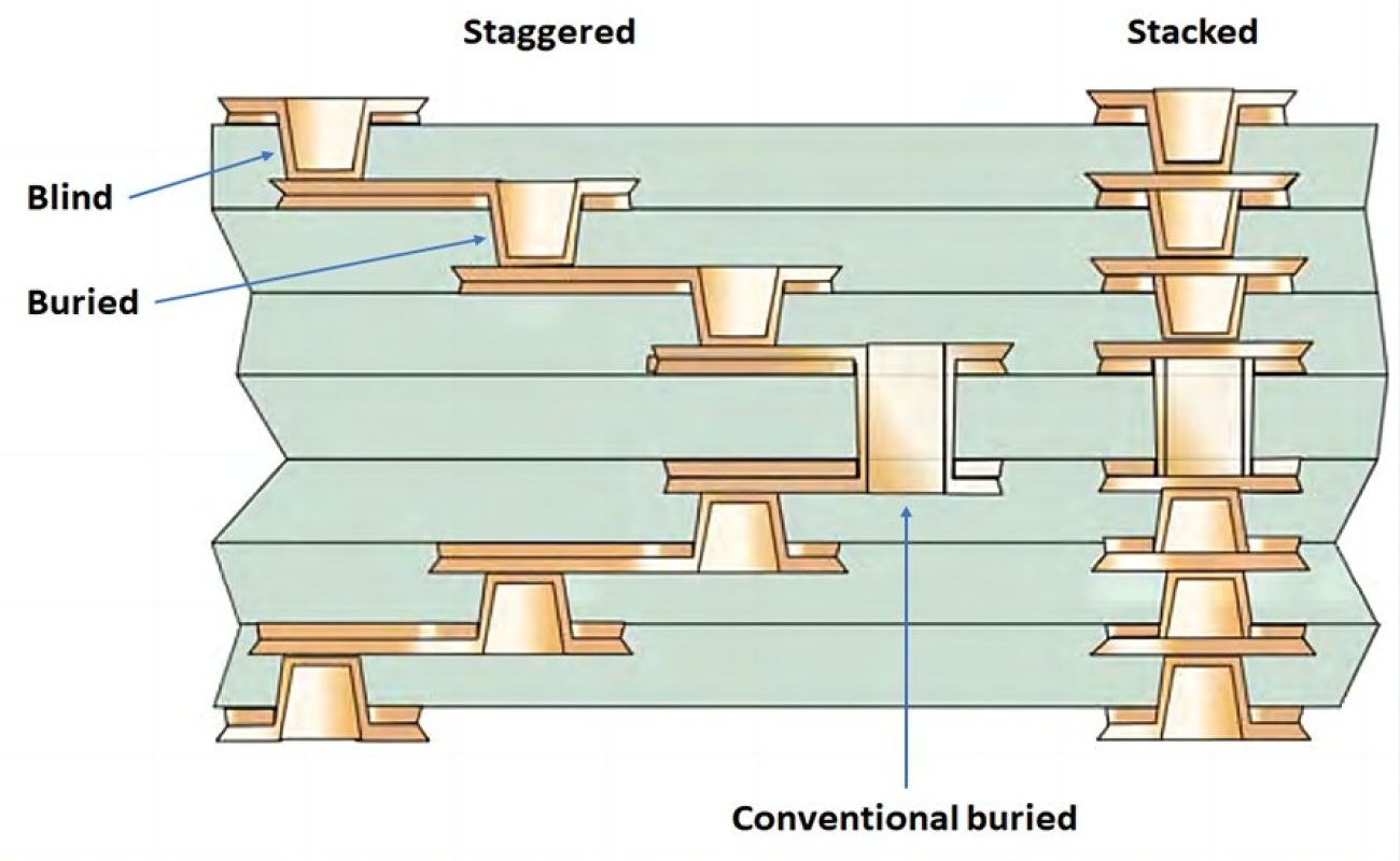
By designing with the plating process in mind, you can avoid defects that compromise electrical performance or reliability. 3. Minimize Via Stacking in HDI PCBsIn HDI PCBs, stacking blind vias or microvias on top of each other is a common technique to connect multiple layers in a small area. However, excessive stacking can create manufacturability issues.
If stacking is unavoidable, ensure precise alignment during design and verify the fabricator's capability to handle such structures.
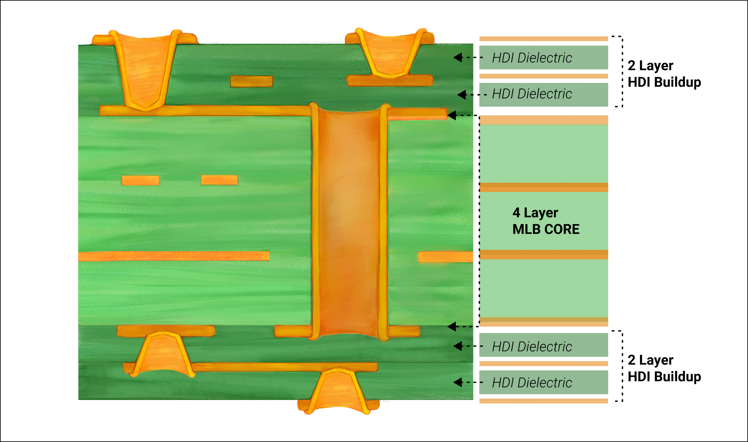
4. Choose the Right Materials for HDI PCBsThe materials used in your PCB design directly impact the manufacturability of blind and buried vias. HDI PCBs often require thin dielectric layers to accommodate microvias, but not all materials are suitable for laser drilling or high-density designs.
Consult with your fabrication team to select materials that balance performance with ease of processing for blind and buried vias. 5. Adhere to Minimum Spacing and Clearance RulesIn high-density designs, spacing between vias, traces, and pads is often tight. However, insufficient clearance can lead to manufacturing defects like short circuits or drilling inaccuracies.
Following these spacing guidelines helps ensure that your design can be fabricated without errors, even with tight layouts.
Common Manufacturability Considerations for Blind and Buried ViasBeyond specific design practices, there are broader manufacturability considerations to keep in mind when working with blind and buried vias in HDI PCBs.
Addressing these considerations early in the design phase can prevent costly redesigns and ensure a smoother transition from design to production.
How to Collaborate with Your Fabrication PartnerOne of the most effective ways to ensure manufacturability is to collaborate closely with your PCB fabrication partner from the start. Share your design files early and discuss specific requirements for blind vias, buried vias, and microvias.
This partnership approach can help catch issues early and ensure your design aligns with production capabilities.
Conclusion: Designing for Success with Blind and Buried ViasDesigning PCBs with blind and buried vias offers incredible opportunities for creating compact, high-performance electronics, especially in HDI applications. However, success depends on prioritizing manufacturability through careful attention to aspect ratios, plating processes, material selection, and spacing rules. By following the best practices outlined in this guide, you can create designs that not only meet technical requirements but also transition smoothly into production. At ALLPCB, we're committed to supporting engineers and designers with resources and expertise to bring their ideas to life. Whether you're working on a complex multilayer board or exploring the potential of microvias, these strategies will help you achieve reliable, cost-effective results. Start applying these tips to your next project and see the difference in both design quality and manufacturing efficiency.
 The Role of Flux in PCB Wave Soldering: Selection, Application, and Residue RemovalMarch 16, 2026PCB wave soldering flux types include rosin, water-soluble, and no-clean options with varying activity levels for oxide removal and solder flow. This guide covers selection criteria, spray foam drop-jet application methods, residue removal processes, and alternatives like nitrogen blanketing to boost joint reliability and yields for engineers. Article Achieving Uniform Solder Fillets in PCB Wave Soldering: Process ControlMarch 16, 2026Achieve uniform solder fillets in PCB wave soldering with process control strategies. Optimize flux, preheat, wave height, conveyor speed for consistent fillet shape, height, and wetting balance. Includes visual inspection tips and troubleshooting for reliable through-hole assemblies. Boost quality in production. Article Optimizing Conveyor Speed for Efficient PCB Wave SolderingMarch 16, 2026Learn PCB wave soldering conveyor speed calculation to manage dwell time, immersion depth, and throughput effectively. Electric engineers get practical steps, best practices, and troubleshooting tips for higher process efficiency and fewer defects in wave soldering operations. Article Understanding IPC Standards for PCB Surface Finishes: Ensuring Quality and ComplianceMarch 11, 2026Understand IPC standards IPC 4552 ENIG and IPC 4553 immersion silver for PCB surface finishes. Ensure compliance, enhance solderability, and prevent common defects to achieve reliable, high quality circuit boards. Article Miniaturization Challenges in PCB AssemblyMarch 11, 2026Navigate the complexities of high density interconnect PCB assembly and precise component placement. Learn to tackle miniaturization challenges, from tiny part handling to thermal stress, ensuring robust and reliable electronics. Article High Speed Routing Techniques: PCBMarch 11, 2026Master high speed routing in PCBs to ensure signal integrity and minimize electromagnetic interference. Learn essential techniques for robust designs, from controlled impedance to differential pair strategies. Prevent performance issues and achieve reliable electronics. ArticleGet Instant PCB |